Скачать с ютуб Working of npn transistor ‖ Emitter forward biased and Collector reverse biased в хорошем качестве
Working of npn transistor ‖ Emitter forward biased and Collector reverse biased
2 года назад
Из-за периодической блокировки нашего сайта РКН сервисами, просим воспользоваться резервным адресом:
Загрузить через dTub.ru Загрузить через ycliper.com Загрузить через ClipSaver.ruСкачать бесплатно Working of npn transistor ‖ Emitter forward biased and Collector reverse biased в качестве 4к (2к / 1080p)
У нас вы можете посмотреть бесплатно Working of npn transistor ‖ Emitter forward biased and Collector reverse biased или скачать в максимальном доступном качестве, которое было загружено на ютуб. Для скачивания выберите вариант из формы ниже:
Загрузить музыку / рингтон Working of npn transistor ‖ Emitter forward biased and Collector reverse biased в формате MP3:
Роботам не доступно скачивание файлов. Если вы считаете что это ошибочное сообщение - попробуйте зайти на сайт через браузер google chrome или mozilla firefox. Если сообщение не исчезает - напишите о проблеме в обратную связь. Спасибо.
Если кнопки скачивания не
загрузились
НАЖМИТЕ ЗДЕСЬ или обновите страницу
Если возникают проблемы со скачиванием, пожалуйста напишите в поддержку по адресу внизу
страницы.
Спасибо за использование сервиса savevideohd.ru
Working of npn transistor ‖ Emitter forward biased and Collector reverse biased
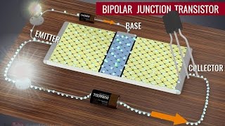
npn transistor in which one p-type material is placed between two n-type materials is known as NPN transistor. The NPN transistor amplifies the weak signal enter into the base and produces strong amplify signals at the collector end. In NPN transistor, the direction of movement of an electron is from the emitter to collector region due to which the current constitutes in the transistor. Such type of transistor is mostly used in the circuit because their majority charge carriers are electrons which have high mobility as compared to holes. The NPN transistor has two diodes connected back to back. The diode on the left side is called an emitter-base diode, and the diodes on the left side are called collector-base diode. These names are given as per the name of the terminals. npn-transistorThe NPN transistor has three terminals, namely emitter, collector and base. The middle section of the NPN transistor is lightly doped, and it is the most important factor of the working of the transistor. The emitter is moderately doped, and the collector is heavily doped. The circuit diagram of the NPN transistor is shown in the figure below. The forward biased is applied across the emitter-base junction, and the reversed biased is applied across the collector-base junction. The forward biased voltage VEB is small as compared to the reverse bias voltage VCB. The emitter of the NPN transistor is heavily doped. When the forward bias is applied across the emitter, the majority charge carriers move towards the base. This causes the emitter current IE. The electrons enter into the P-type material and combine with the holes. The base of the NPN transistor is lightly doped. Due to which only a few electrons are combined and remaining constitutes the base current IB. This base current enters into the collector region. The reversed bias potential of the collector region applies the high attractive force on the electrons reaching collector junction. Thus attract or collect the electrons at the collector. The whole of the emitter current is entered into the base. Thus, we can say that the emitter current is the sum of the collector and the base current.
Comments